
Артикул:
Stock #16-856
Нашли дешевле?
Характеристики
Coating
—
Uncoated
Substrate
—
Single Crystal Silicon
Surface Quality
—
60-40 (within CA)
Clear Aperture CA (mm)
—
24.00 x 24.00
Type
—
Nanopatterned Silicon Stamp
RoHS
—
Compliant
Все характеристики
Цена действительна только для интернет-магазина и может отличаться от цен в розничных магазинах
Learn More
Product Family Description
- Nanoscale-Textured Grooved Surfaces
- Variable Groove Period and Groove Depth
- Ideal for Nanophotonics Research Applications
II-VI LightSmyth™ Nanopattern Silicon Stamps consist of nanoscale-textured surfaces patterned on single-crystal silicon substrates. Through reactive ion etching, linear grooves with a trapezoidal cross-section are etched into the substrate surface, resembling conventional gratings. The etching process enables different period and depth specifications for these grooves, as well as more complex patterns such as lattices. II-VI LightSmyth™ Nanopattern Silicon Stamps are ideal for nanophotonics research applications in the fields of optics and photonics, biology, chemistry, nanoimprinting, and microfluidics.
Документы
Coating
Uncoated
Substrate
Single Crystal Silicon
Surface Quality
60-40 (within CA)
Clear Aperture CA (mm)
24.00 x 24.00
Type
Nanopatterned Silicon Stamp
RoHS
Compliant
Construction
RIE Grating
Thickness (mm)
0.68 ±0.05
Model Number
1304077
Dimensions (mm)
25.00 x 25.00
Length (mm)
25.00
Width (mm)
25.00
Period (nm)
855 ±42.75
Groove Depth (nm)
200 ±30
Line Width (nm)
425
Отзывы
Оставить отзыв
Загрузка отзывов...
Technical Information

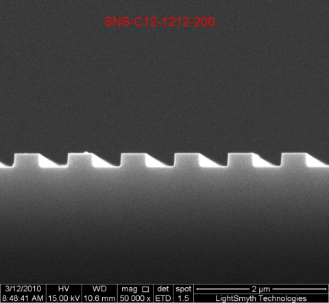
SEM Image of 855nm, 200nm Groove Depth Linear Silicon Nanostamps (Cross Section)
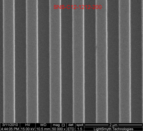
SEM Image of 855nm, 200nm Groove Depth Linear Silicon Nanostamps (Top Down)
Вам также может понравиться
